


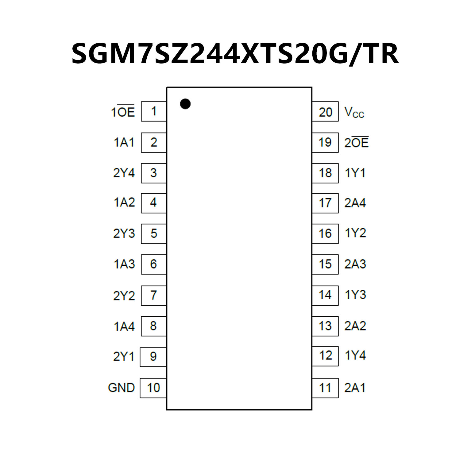
 SGM7SZ244.pdf
? Wide Operating Voltage Range: 1.8V to 5.0V
? High-Current Outputs Drive Up to 15 LSTTL
Loads
? 3-State Outputs Drive Bus Lines or Buffer
Memory Address Registers
? Low Power Consumption, ICC: 25μA (MAX)
? Typical tPD = 8.9ns at 5.0V
? ±20mA Output Drive at 5.0V
? Low Input Current: ±8μA (MAX)
? -40℃ to +125℃ Operating Temperature Range
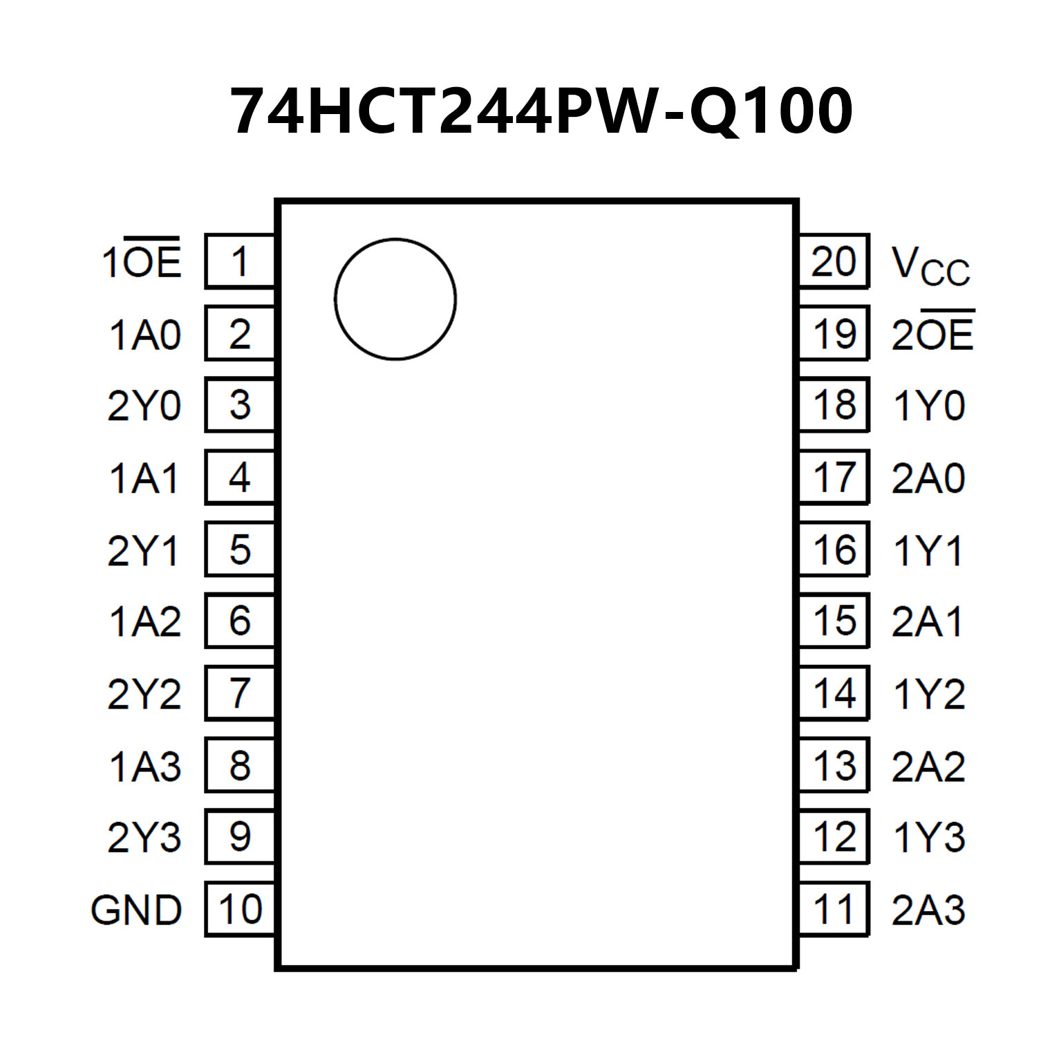
? Available in a Green TSSOP-20 Package
? Automotive product qualification in accordance with AEC-Q100 (Grade 1)
? Specified from -40 °C to +85 °C and from -40 °C to +125 °C
? Wide supply voltage range from 2.0 to 6.0 V
? CMOS low power dissipation
? High noise immunity
? Latch-up performance exceeds 100 mA per JESD 78 Class II Level B
? Input levels:
For 74HC244-Q100: CMOS level
For 74HCT244-Q100: TTL level
? Octal bus interface
? Non-inverting 3-state outputs
? Complies with JEDEC standards:
JESD8C (2.7 V to 3.6 V)
JESD7A (2.0 V to 6.0 V)
? ESD protection:
MIL-STD-883, method 3015 exceeds 2000 V
HBM JESD22-A114F exceeds 2000 V
MM JESD22-A115-A exceeds 200 V (C = 200 pF, R = 0 Ω)
? Multiple package options
? DHVQFN package with Side-Wettable Flanks enabling
Automatic Optical Inspection (AOI) of solder joints